
Micro-Precision Laser Marking for Electronics & PCBs
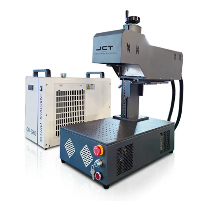
Laser marking systems (UV, fiber, and CO₂) can produce permanent, high-contrast QR codes and serial numbers with micrometer-level precision.
The Fabrication Challenge
Traceability is the backbone of the global electronics industry. Semiconductors, PCBs, and sensors require highly legible, microscopic tracking codes. Relying on traditional continuous inkjet (CIJ) printing or low-quality thermal engraving introduces fatal supply chain and manufacturing risks
Ink Degrades in SMT Reflow Ovens
Inkjet printing is highly vulnerable to the harsh environments of electronics manufacturing. When a PCB goes through a wave soldering machine or chemical washdown, traditional ink easily smudges, fades, or completely dissolves. A microchip with an unreadable 2D matrix code destroys cradle-to-grave traceability, resulting lead to massive recall liabilities
Thermal Damage to Sensitive Silicon (HAZ)
Using the wrong type of laser creates a massive Heat Affected Zone (HAZ). The thermal conduction melts the plastic packaging and can literally fry the microscopic circuits immediately beneath the surface of the die, reducing manufacturing yields and causing premature field failures.
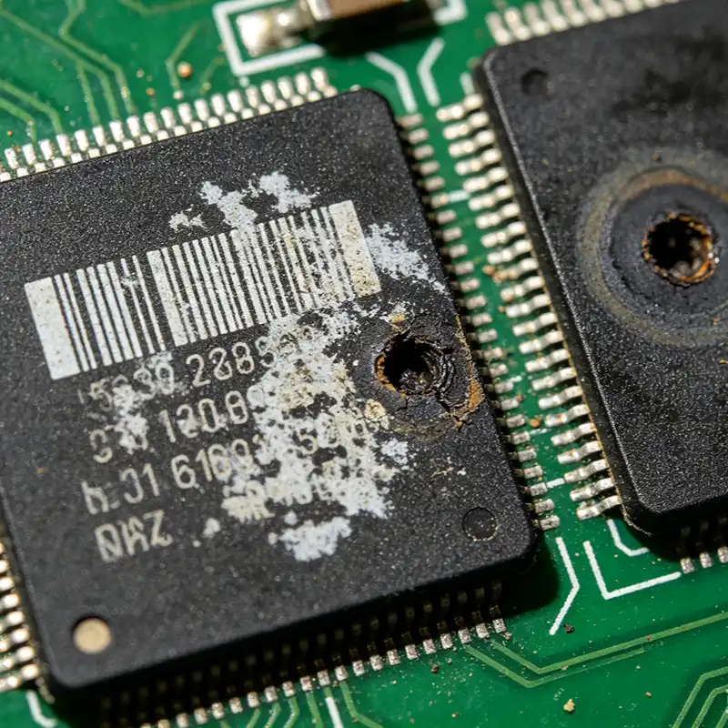
he Counterfeit Component Threat
Ink is superficial. It can be easily wiped away with isopropyl alcohol or chemical solvents by grey-market counterfeiters who reprint fake specifications on inferior chips. Without permanent, sub-surface part marking, OEMs cannot defend their brand integrity or track the true origin of a failed aerospace or automotive ECU component.
Why Electronics Need Laser-Marking?
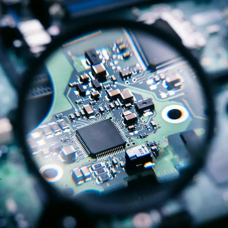
CCD Vision Auto-Positioning
Electronic components shrink every year. JCT laser marking systems integrate ultra-high-resolution CCD cameras .They scan the PCB or IC tray as it enters the marking station. The software identifies fiducial markers, calculates the exact X/Y coordinates and rotational angle, and automatically aligns the laser path—guaranteeing perfect mark placement even if the board is placed slightly askew.
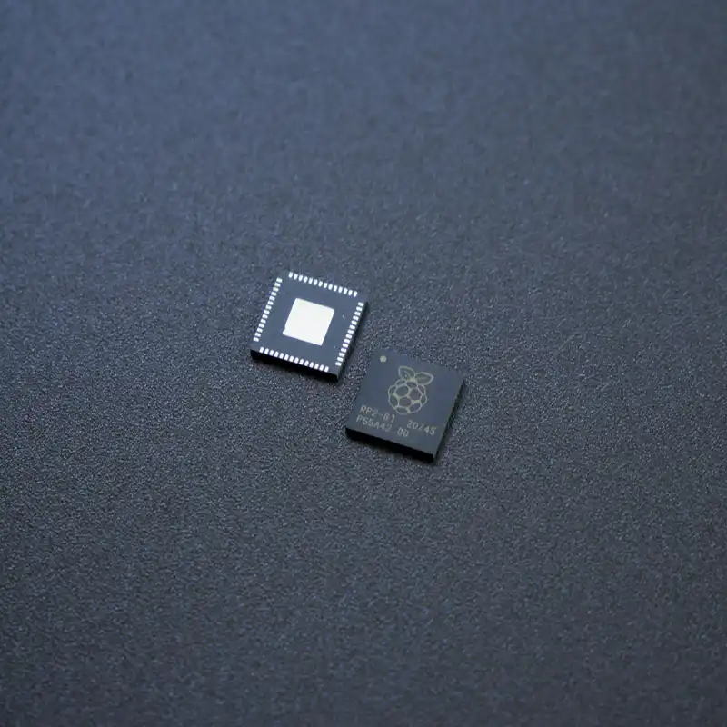
Non-Destructive Micron Marking
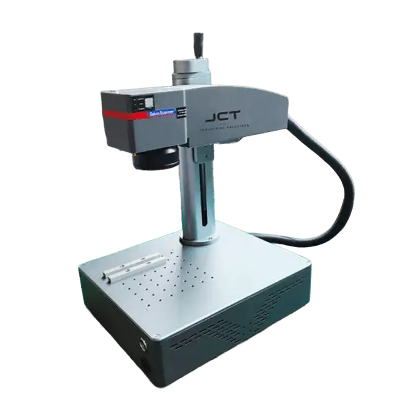
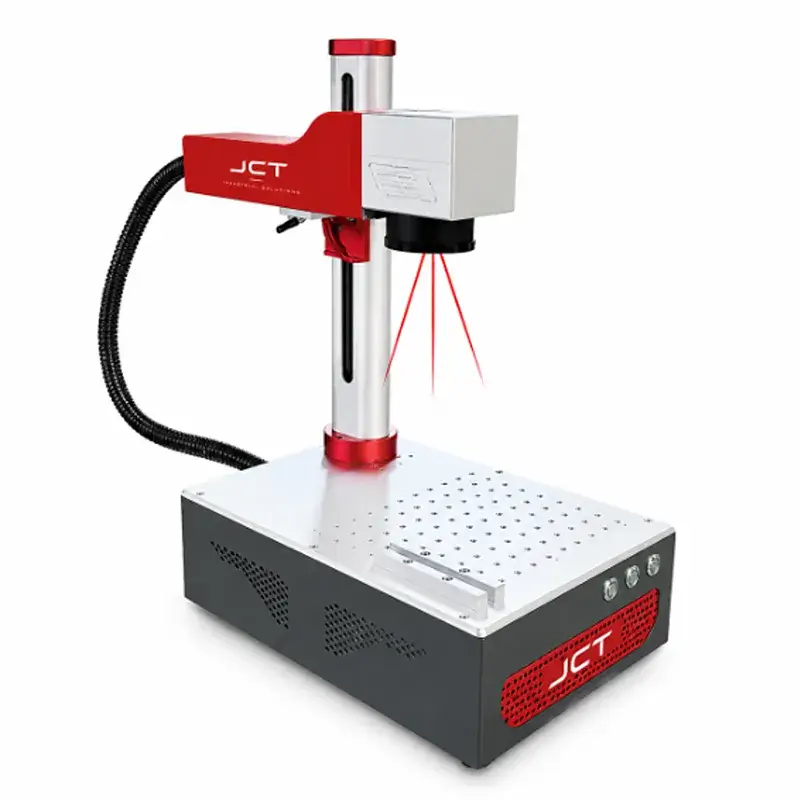
Based on your substrate, the system fires the exact wavelength required (UV, Fiber, or CO2). The laser creates high-contrast alphanumeric texts, logos, and QR codes in milliseconds. The beam spot can be focused down to 10 microns, it can enable perfectly legible data to be etched onto the thinnest capacitors and IC packages without altering their electrical properties.
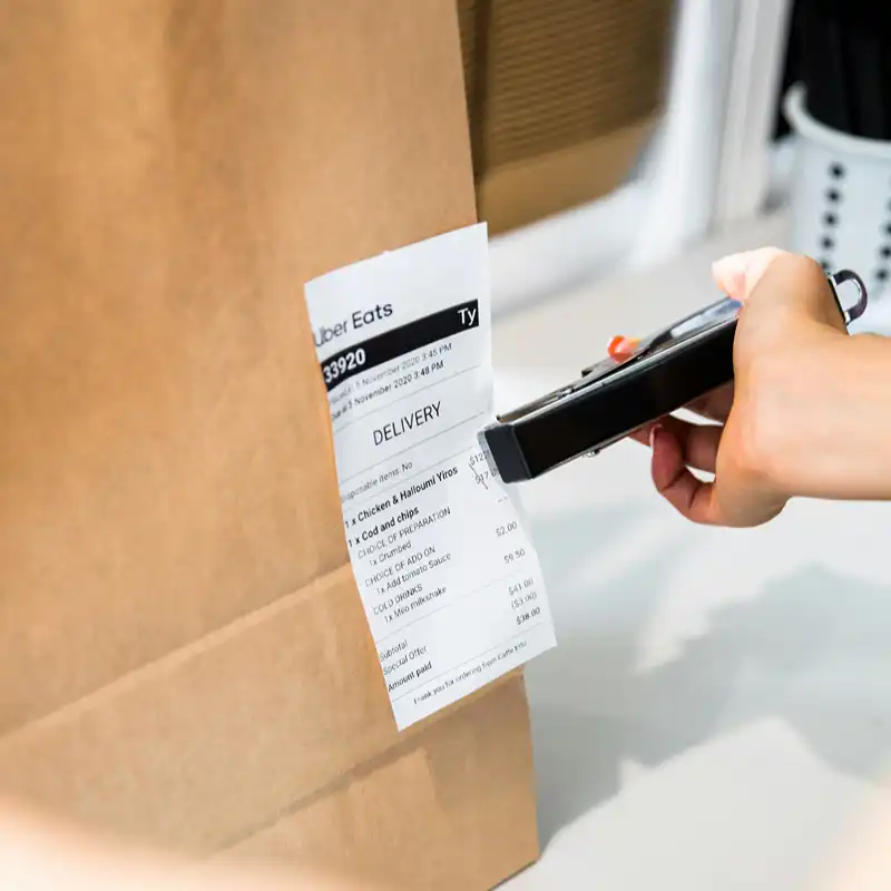
Instant Inline Verification
Traceability is only valuable if the code can be read. Immediately after marking, integrated coaxial scanners or secondary vision systems read the 2D code. It verifies the data against your factory MES/ERP database, grades the contrast quality, and instantly flags any defective components before they proceed down the SMT line
or Electronic Substrates We CAN Supply
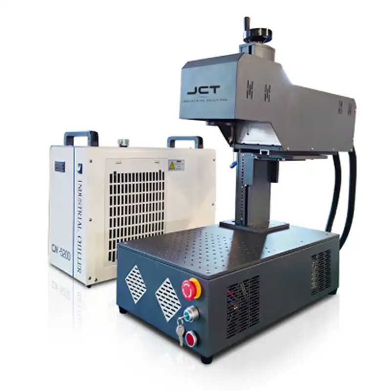
Silicon wafers, high-density PCBs, delicate IC plastic packaging, smartphone glass, and ceramic substrates.
The ultimate “Cold Marking” technology. With an infinitely small focal spot, it produces exceptionally high-contrast, soot-free marks on heat-sensitive components without altering their electrical resistance. It is the absolute standard for premium semiconductor traceability
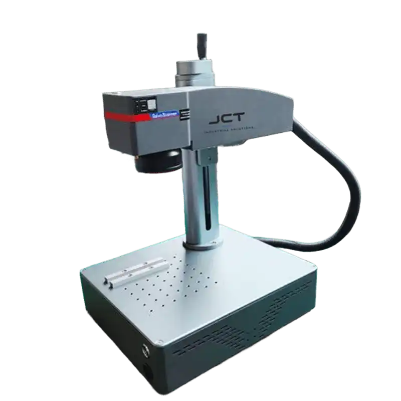
Copper PCB traces, aluminum heat sinks, metal ECU housings, stainless steel sensor bodies, and gold-plated connectors
Unrivaled speed and depth on metals. Employs photothermal ablation to engrave permanent, unalterable serial numbers into metal components that survive harsh automotive and aerospace environments. Features a lifespan exceeding 100,000 hours with zero consumables
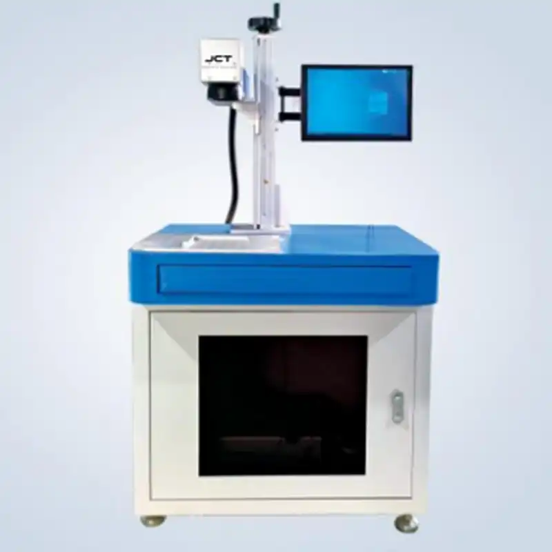
Standard FR4 PCB substrates, paper packaging, polycarbonate electronic housings, and ABS control panels.
The most cost-effective solution for non-metals. Rapidly changes the surface color of electronic plastic casings to create high-visibility logos and QR codes. Easily integrates into automated conveyor belts for high-speed, on-the-fly marking of consumer electronic exteriors.
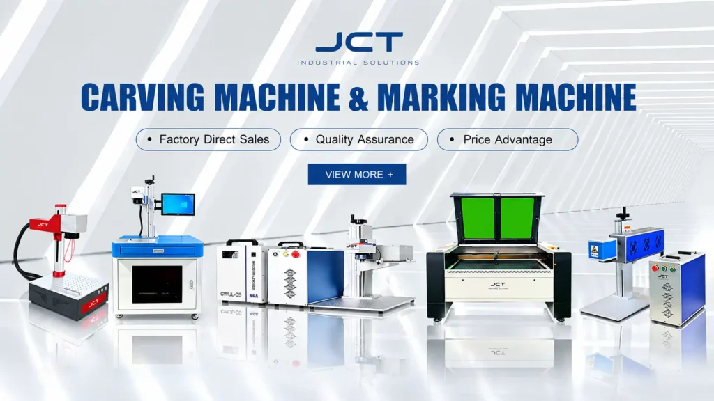
WHO WE ARE?
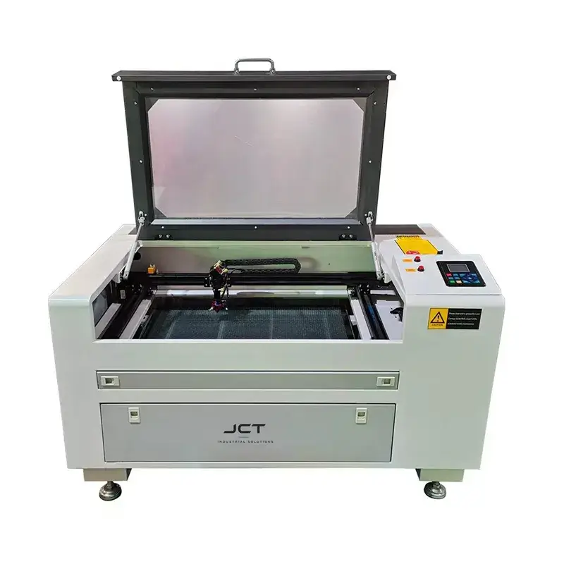
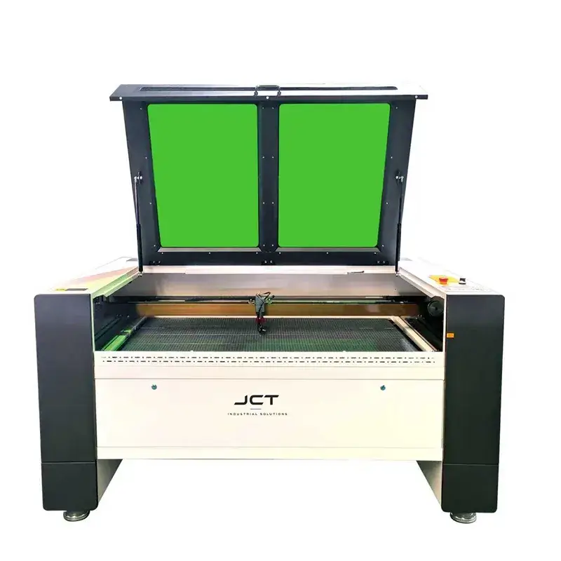
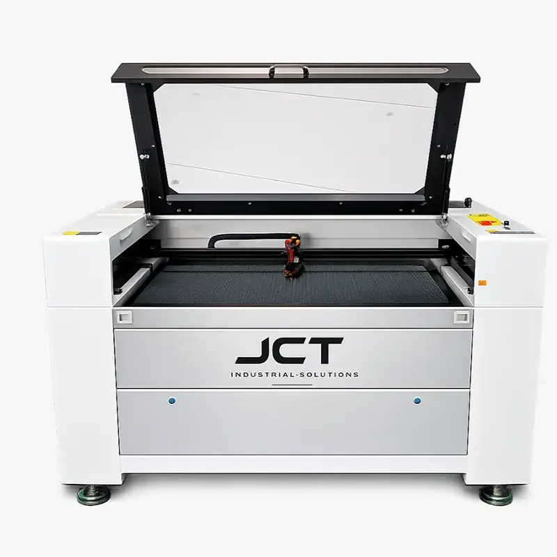
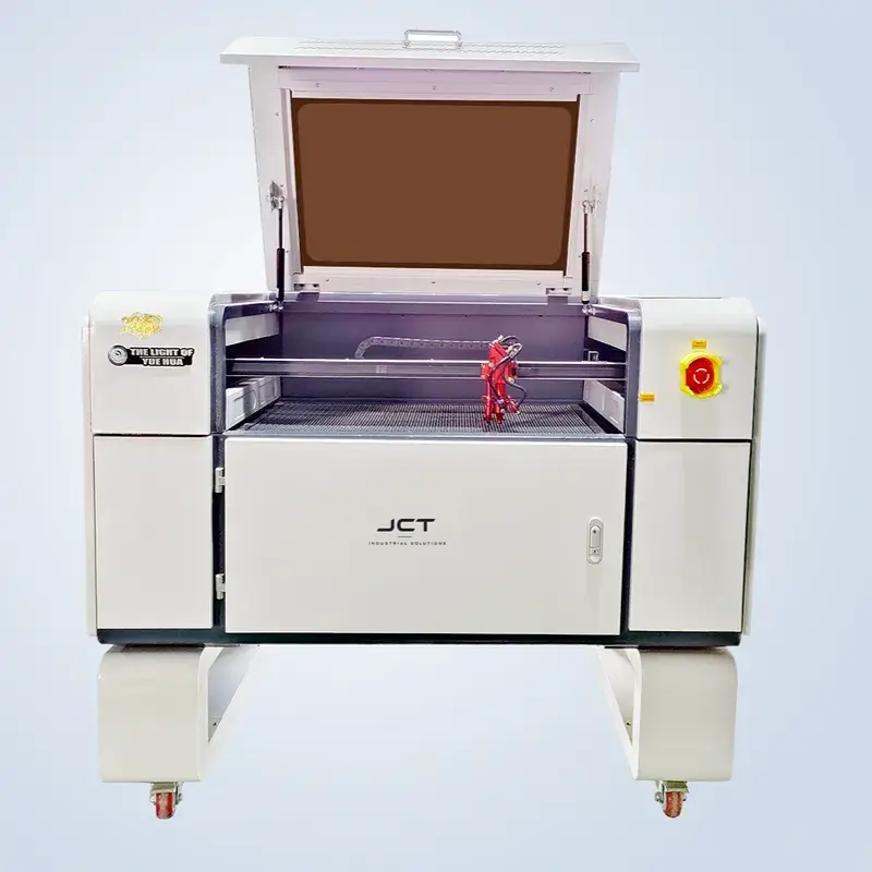
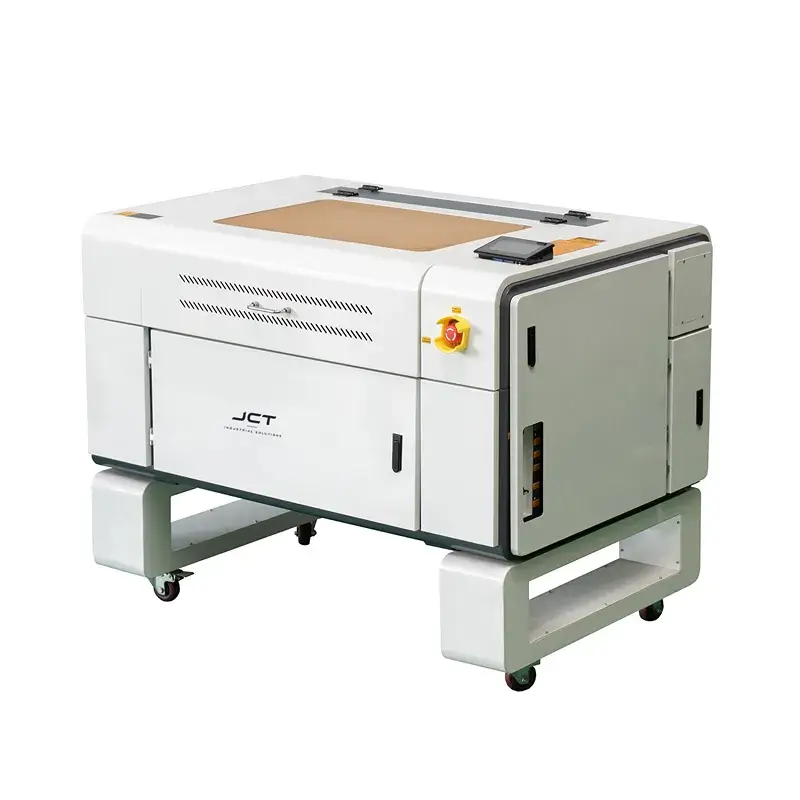
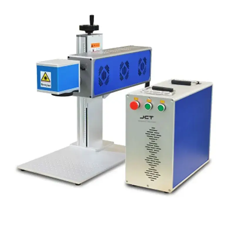
We are the source factory of CO2 laser engraving machines.
We offer both square rail and embedded rail models. We build work areas from 30cm up to 160cm to fit different workpiece sizes. Customization is always welcome to match your exact needs.
Based in China, our machines have reached over 50+ countries, including Europe, Central Asia, the Middle East, Southeast Asia, and Latin America.
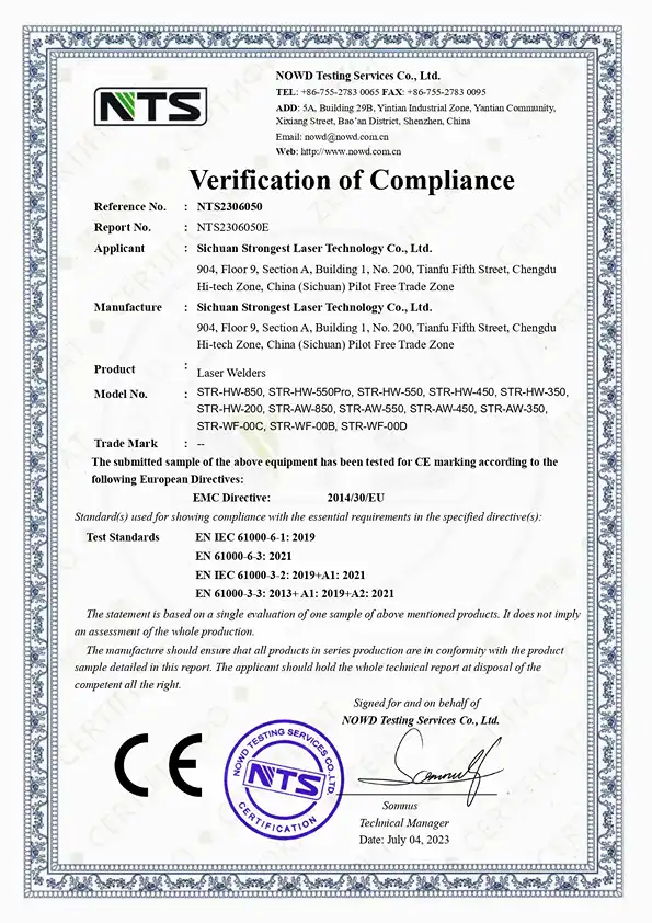
We hold multiple product patents. We are ISO9001 and CE certified.
Choose JCT. Choose a lifelong partner.
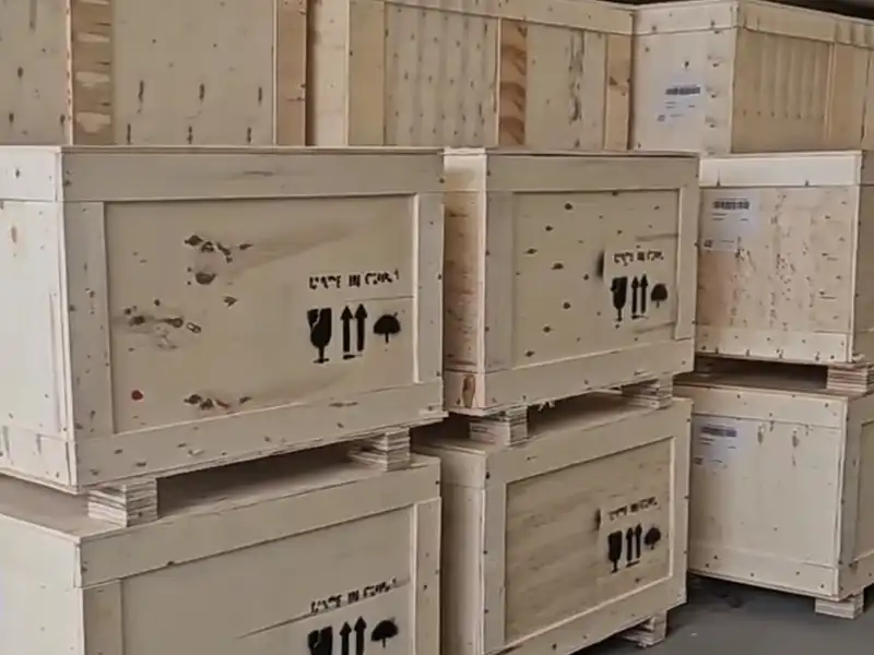
OUR CORE ADVANTAGES
Why Choose Us
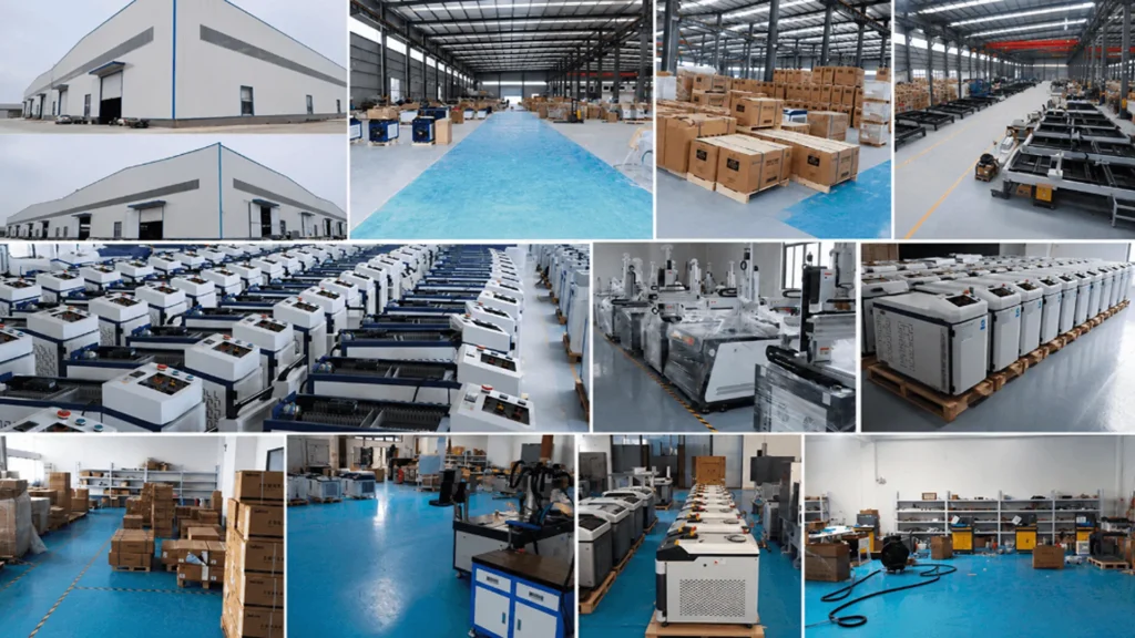
With over 10 years of rich industry experience, we are committed to served as a comprehensive technology manufacturer partner worldwide.We understand that your successful product relies on two core pillars: efficient manufacturing and uncompromising quality control.As a result, we offer a dual-core product line: first, laser and FAB solutions that ensure efficient manufacturing; and second, environmental test chambers for testing the performance of your products—all designed to address your specific industry issues and challenges.
Industry-Specific Customization
Whether you’re in the sheet metal or metalworking industries, or specialize in testing semiconductors and automotive electronics, our equipments all can be customized to meet your specific needs. We don’t just sell standard machines—we provide precise solutions that perfectly match your material and environmental requirements.
High-Efficiency Manufacturing
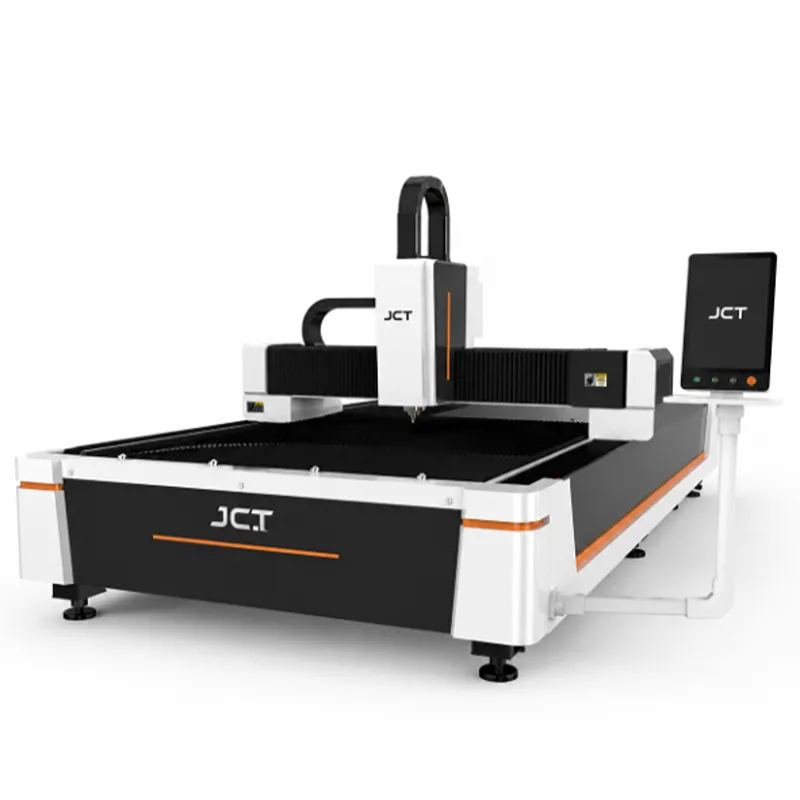
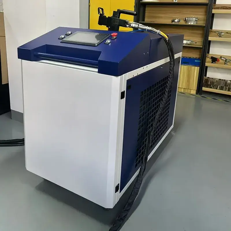
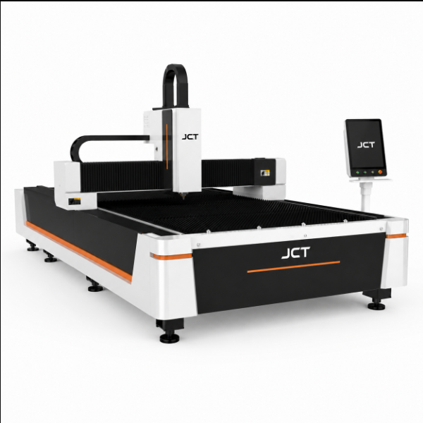
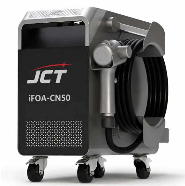
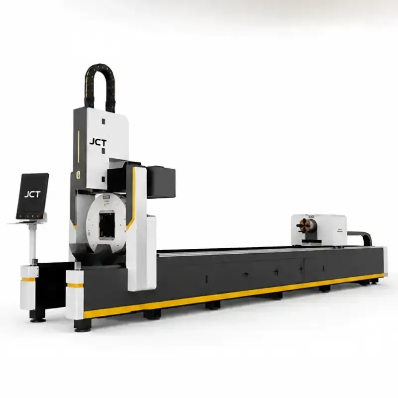
In the manufacturing process, time is your most valuable treasure. We offer fiber laser welding, cutting, and cleaning,etc solutions . All of them can provide deep penetration, distortion-free welding, precise cutting, and efficient cleaning for sheet metal and various types of metal processing.
Compliance and Quality Control
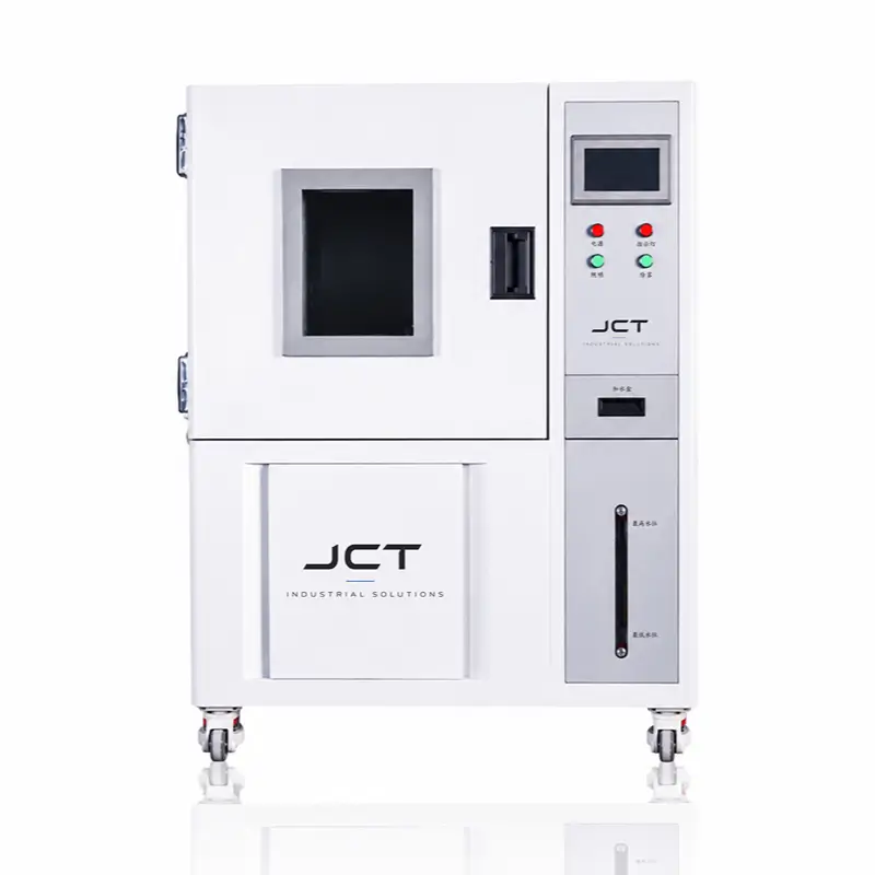
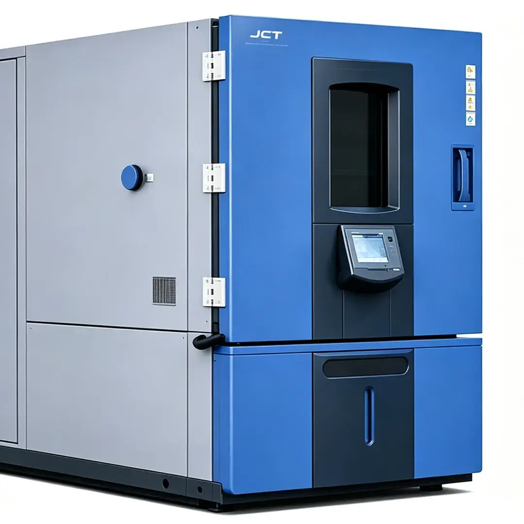
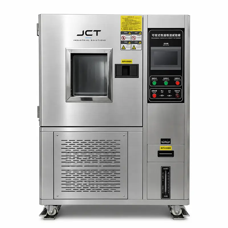
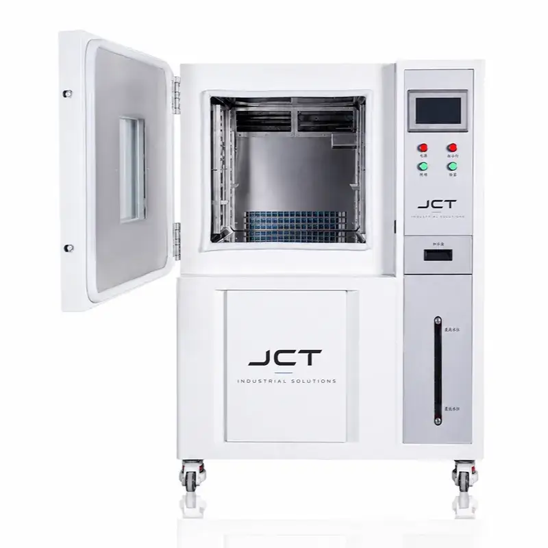
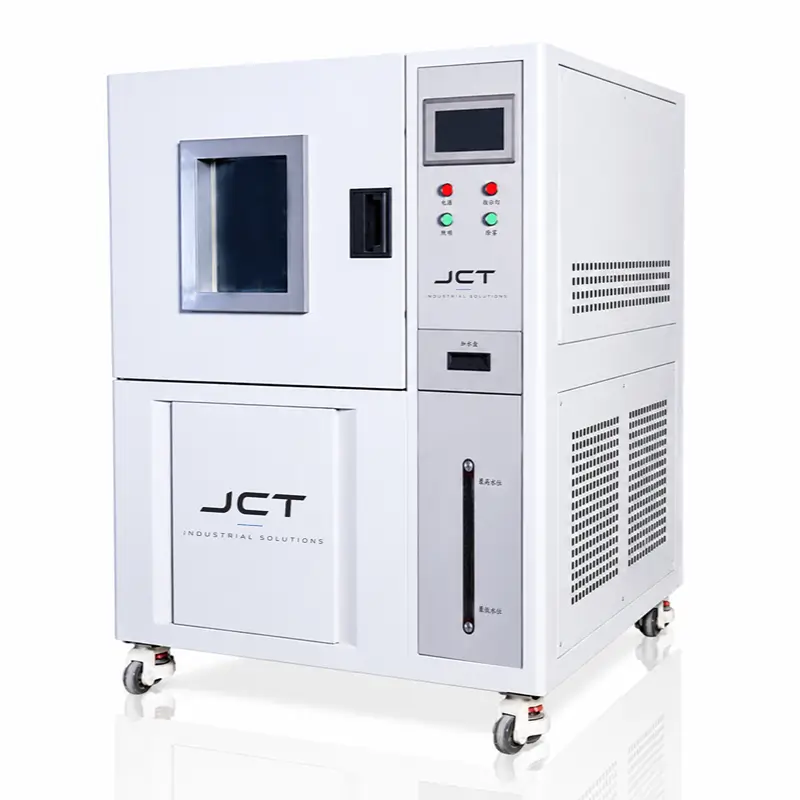
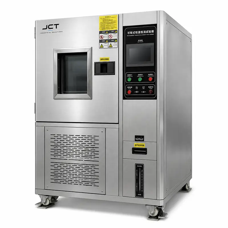
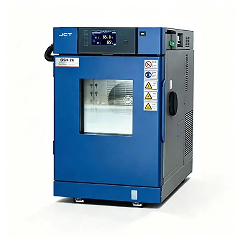
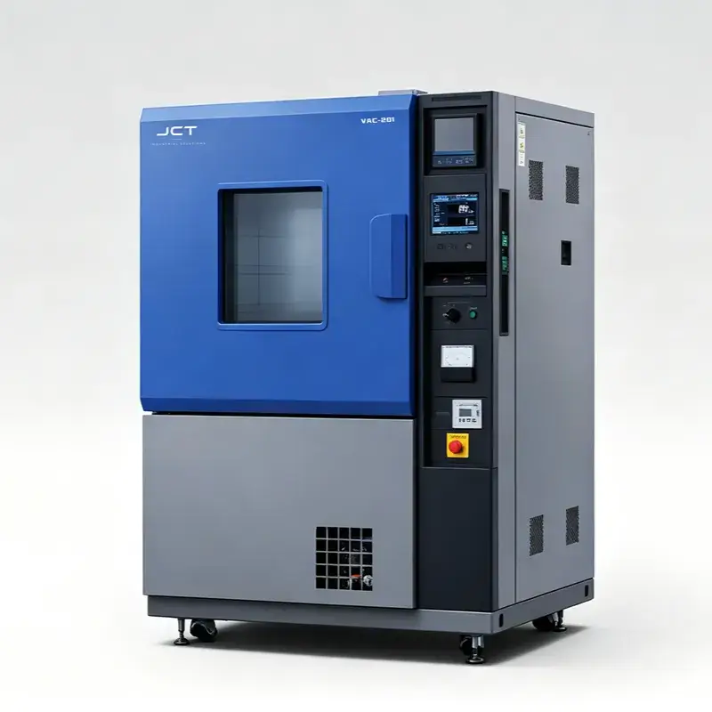
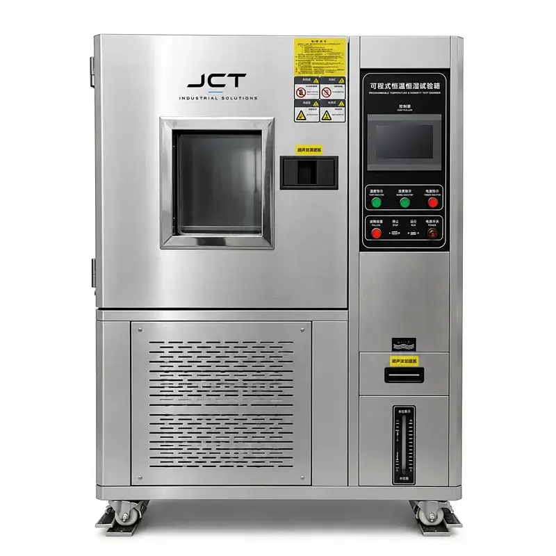
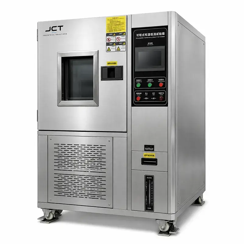
We ensure that your finished products can pass the most rigorous environmental testing. Our environmental test chambers help you meet strict global standards such as JEDEC, AEC-Q100, and key battery safety certifications, all these can shorten your R&D cycle and eliminating the risk of customer returns .
10+ Years & Global Support
With over a decade of technical expertise and a robust supply chain, we guarantee on-time delivery worldwide. More importantly, our engineering team will provide lifetime technical support, and we are committed to being your stable and reliable partner and friend for life.
PREMIUM COMPONENTS ASSURANCE
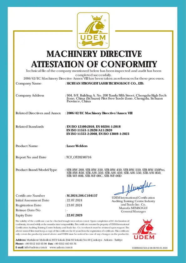
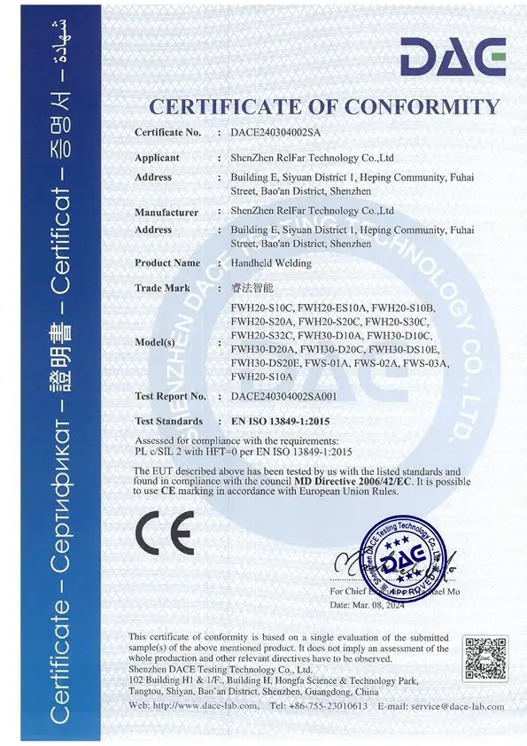
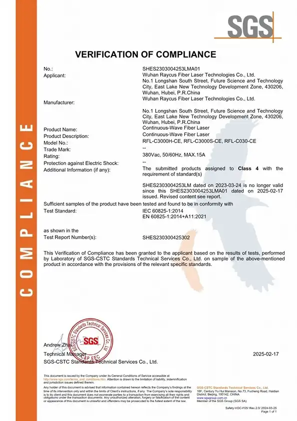
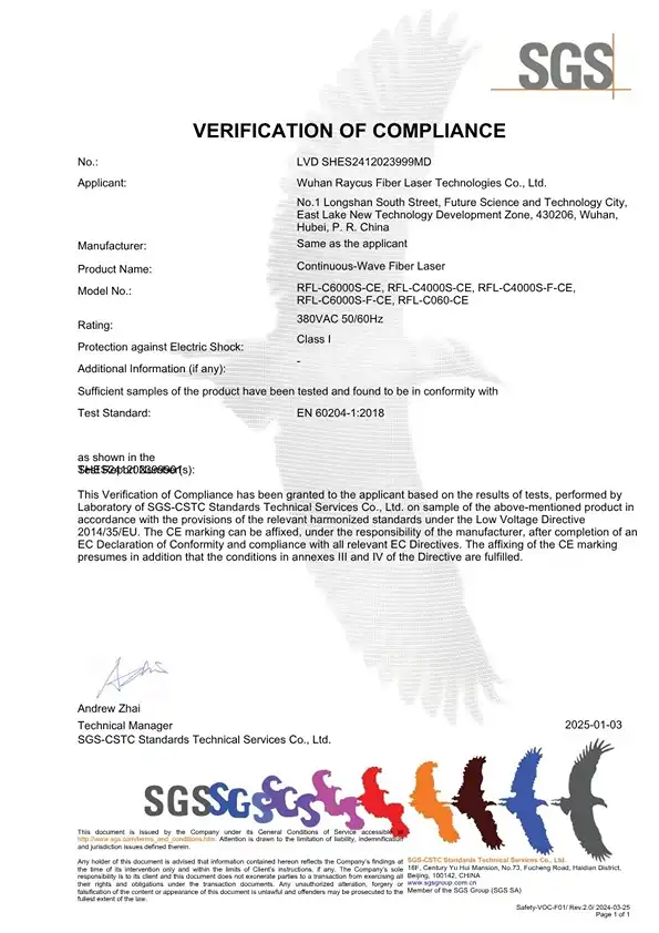
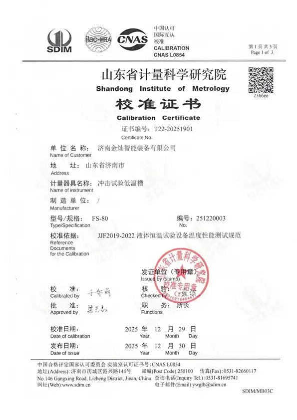
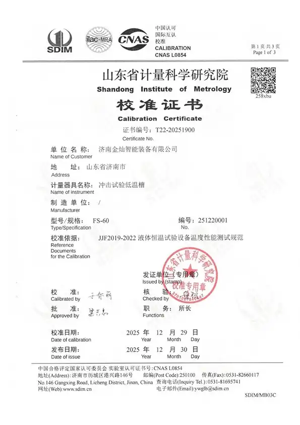
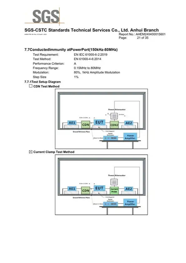
Certified to Global Leading Standards
Reliability starts at the core. The key components that power our equipment—from the laser source to even the smallest electronic components—have all been certified to meet the world’s most stringent international standards.
GLOBAL PARTNERSHIPS
Trusted by Industry Leaders Worldwide
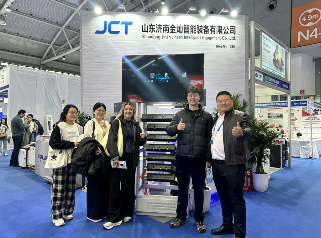
We take pride in powering the success of top-tier global manufacturers, research institutions, and industrial leaders. Our advanced laser and testing solutions are trusted worldwide to deliver uncompromising quality and peak performance.



FAQ
Q1: We use inkjet printers for PCBs, but the ink washes off during flux cleaning. Will laser fix this?
Yes
Ink is an additive layer that sits on top of the material, making it vulnerable to chemicals and heat. Laser marking is a subtractive process—it microscopically alters or vaporizes the top layer of the material itself. The mark is physically integrated into the component and cannot be washed off, ensuring lifetime traceability.
Q2: We manufacture sensitive microchips. Won't a laser burn through the plastic packaging and damage the silicon?
Not if you use the correct wavelength. A standard Fiber laser might cause thermal damage. However, our UV (Ultraviolet 355nm) laser utilizes “cold ablation.” It breaks chemical bonds without generating significant heat, It allows you to mark ultra-thin IC packaging without affecting the underlying silicon die.
Q3: Can a laser mark QR codes small enough to fit on a tiny 0402 SMD capacitor?
Absolutely. Our UV and Fiber lasers can achieve a focal spot size of less than 10 microns. We can consistently generate crisp, high-contrast, machine-readable 2D DataMatrix codes They are microscopic, fitting easily onto the smallest Surface Mount Devices
Q4: Which laser do I need: UV, Fiber, or CO2?
It depends entirely on the substrate material.
- UV:Best for delicate plastics, silicon, glass, and PCBs where heat damage is a concern (Cold Marking).
- Fiber:Best for bare metals, copper pins, and aluminum heat sinks (High-contrast metal engraving).
- CO2:Best for standard FR4 PCB boards, paper labels, and thick non-metal housings
- Tell us your material, and we will test it for free.
Q5: Can the laser generate unique serial numbers or pull data from our database?
Yes. Our control software (e.g., EZCAD3 or custom MES software interfaces) integrates directly with your factory’s ERP, MES, or Excel databases. It can automatically generate real-time dynamic data, including sequential serial numbers, timestamps, and unique QR codes for every individual chip.
Q6: What maintenance does a laser marker require compared to inkjet?
Laser marking is virtually maintenance-free. There are no ink cartridges to replace, no clogged printheads to soak in toxic MEK solvent, and no messy cleanups. A Fiber laser source can last over 100,000 hours.
Q7: What is the ROI for replacing our inkjet coders with laser markers?
Most electronics manufacturers achieve a full ROI within 6 to 10 months
Related Products
Get a Factory-Direct Custom Quote
Stop struggling with smudged barcodes and toxic chemical solvents.
Tell our application engineers about your specific electronic components, substrate materials (e.g., Silicon, FR4, Aluminum), and SMT line speed. We will run free sample testing and recommend the exact UV, Fiber, or CO2 JCT laser to upgrade your traceability, complete with a factory-direct quote within 12 hours.