
Extreme Environmental Testing for Semiconductor IC Packaging
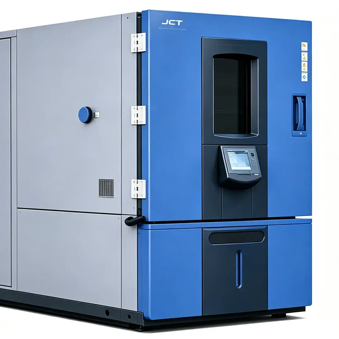
The environmental test chambers can perform rigorous JEDEC moisture immersion tests and demanding thermal shock test protocols
The Fabrication Challenge
Semiconductor packaging is incredibly vulnerable. The epoxy molding compounds (EMC) used to encapsulate silicon dies are hygroscopic—they absorb moisture from the air. When these chips are subjected to the brutal conditions of Surface Mount Technology (SMT) assembly, hidden catastrophic failures occur
The "Popcorn Effect" (Acoustic Emission Failure)
During SMT reflow, temperatures spike up to 260°C in seconds. If an IC package has absorbed ambient moisture, that water instantly flashes into superheated steam. The rapid expansion of this vapor exerts massive internal pressure,then cause the epoxy encapsulation to violently delaminate from the lead frame or die. The package bulges and audibly cracks (like popcorn), completely destroying the microchip from the inside out.
Wire Bond Shear & CTE Mismatch
Microchips rely on hair-thin gold or copper wire bonds to connect the silicon die to the substrate. The silicon, the metal frame, and the epoxy compound all possess vastly different Coefficients of Thermal Expansion (CTE). When subjected to rapid thermal shock, they expand at different rates. This microscopic tug-of-war acts like a pair of scissors, eventually shearing the wire bonds or causing severe solder bump fatigue in Flip-Chip and BGA packages
Infant Mortality (Latent Defects)
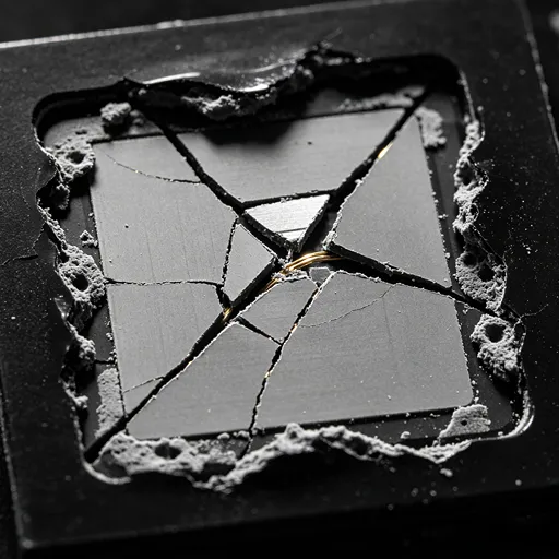
Minor manufacturing flaws—such as oxide layer pinholes or subtle metallization defects—may not fail during initial quality control. However, without High-Temperature Storage Life (HTSL) or burn-in testing, these latent defects manifest early in the field, causing unpredictable operational failures in mission-critical medical, automotive, and aerospace electronics
Why Semiconductor need Climatic testing Chambers?
MSL Moisture Preconditioning
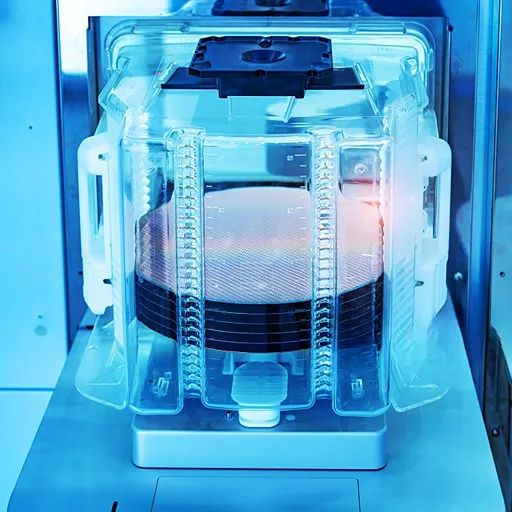
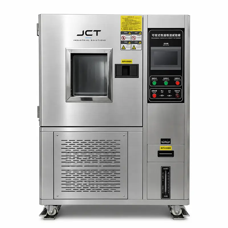
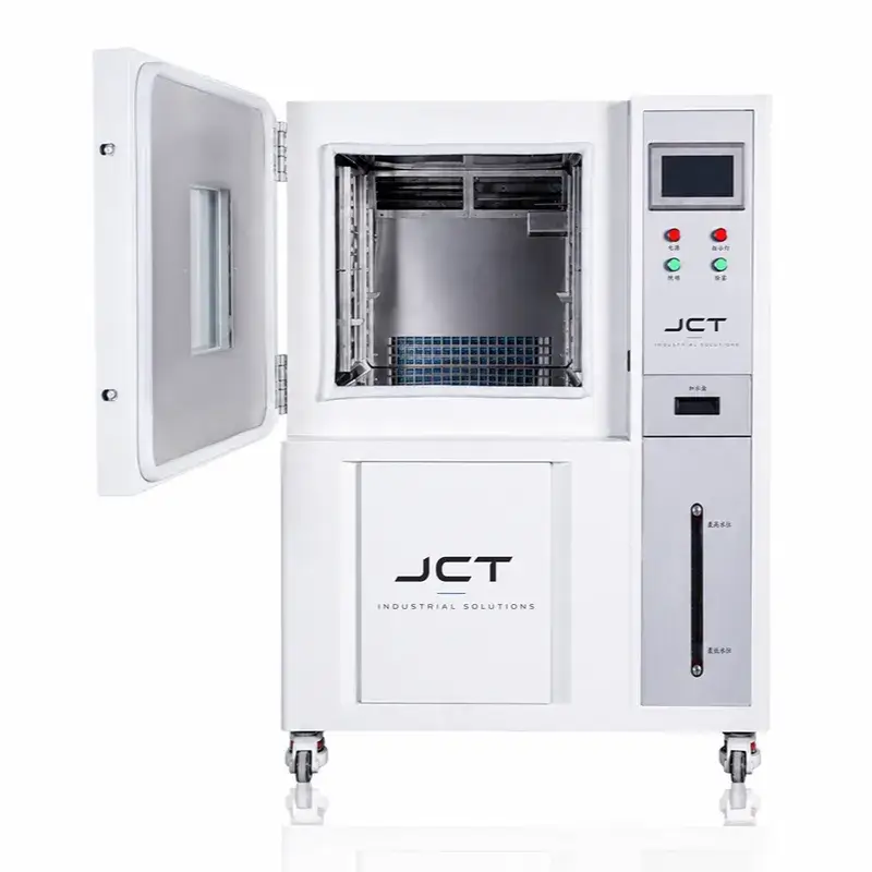
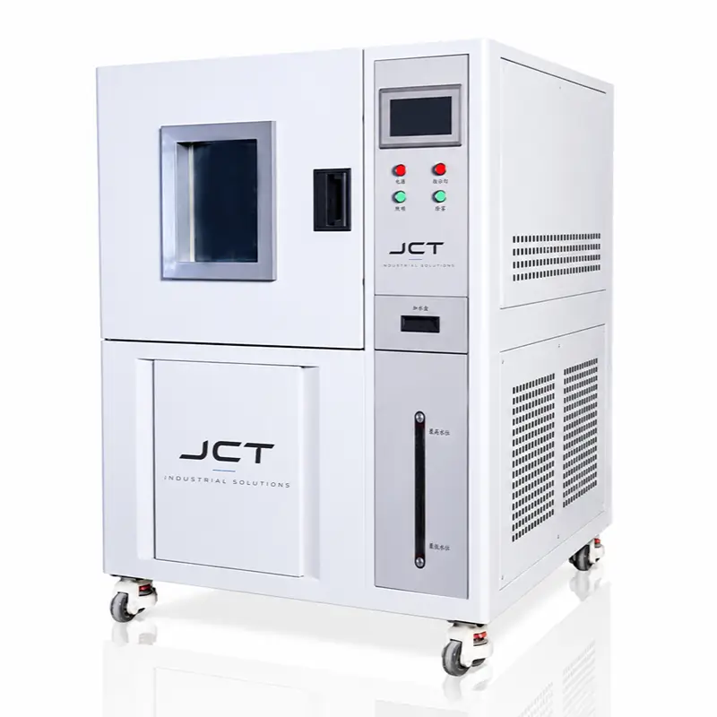
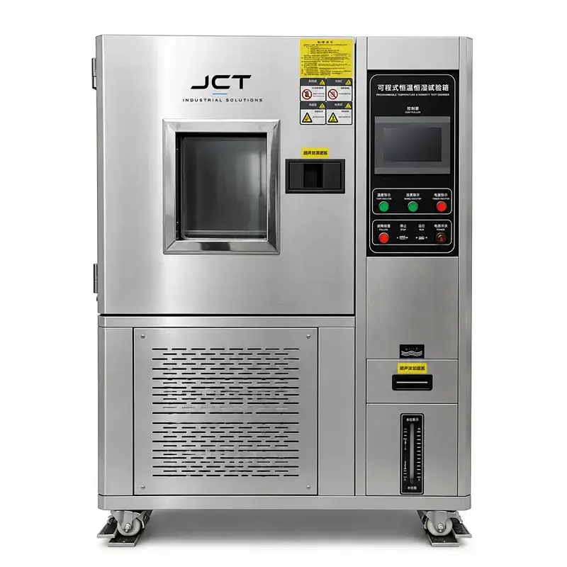
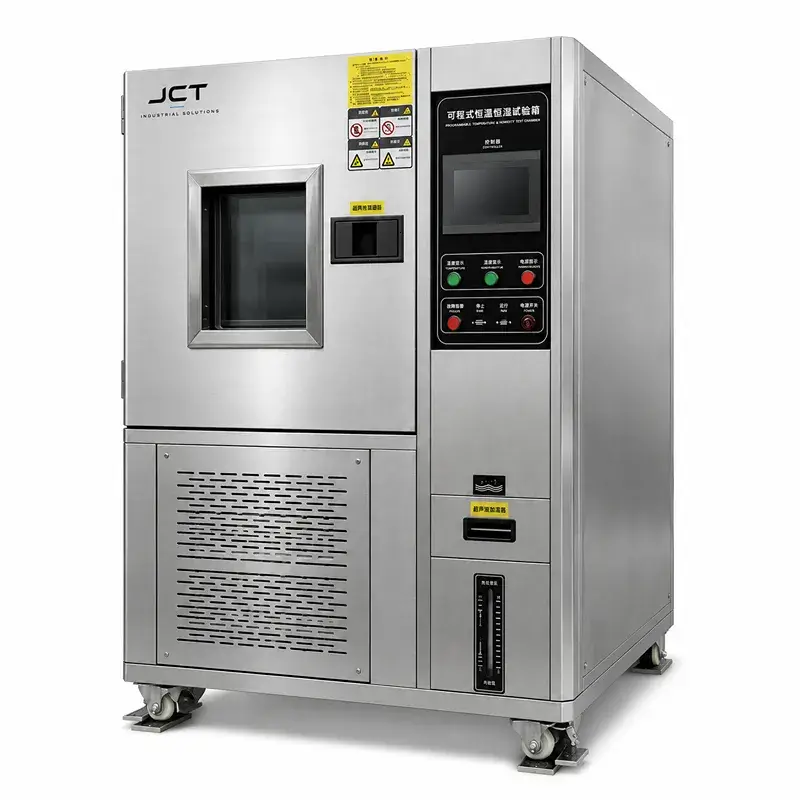
Place Bare ICs into JCT Constant Temperature & Humidity Chambers. By maintaining precise environments (e.g., 85°C / 85% RH for 168 hours for MSL 1), the chamber forces moisture into the epoxy molding compound. This establishes the baseline for how the chip will behave when subjected to the violent heat of the customer’s wave soldering process.
Rapid Thermal Shock Screening
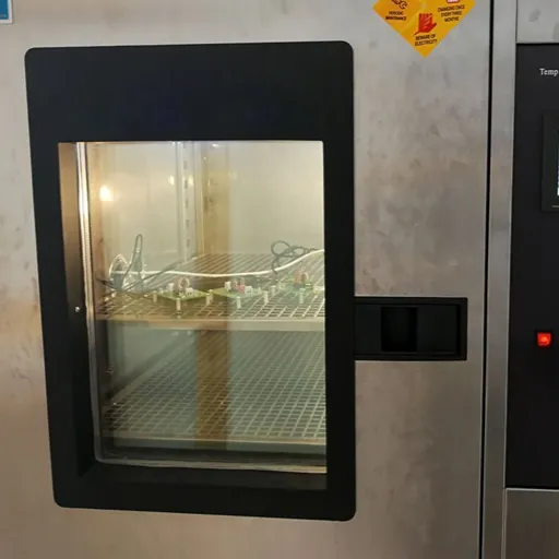
Following the moisture soak and simulated reflow, the IC trays are loaded into a JCT 2-Zone Thermal Shock Chamber. The pneumatic basket drops the chips from a 150°C baking zone instantly into a -65°C freezing zone. This violent thermomechanical stress instantly exposes brittle wire bonds, die cracking, and weak solder bumps
High-Temperature Storage Life
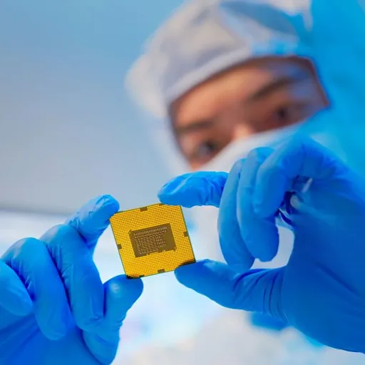
To ensure long-term data retention and operational stability, fully functional ICs are mounted to burn-in boards and placed into a JCT High-Temperature Test Chamber. Baking the chips at 125°C to 150°C for 1,000 hours to accelerates electron migration and dielectric breakdown, ensuring only the most robust silicon ships to the client
for Semiconductor Testing We CAN Supply
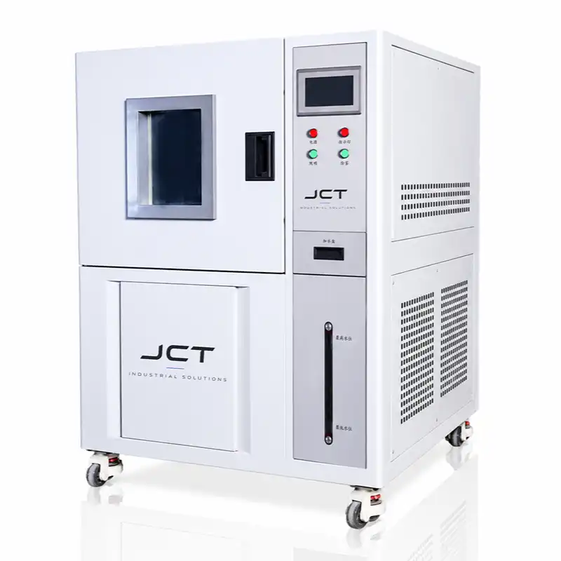
JEDEC Moisture Sensitivity Level (MSL) soaking, HAST (Highly Accelerated Stress Test) preconditioning, and shelf-life simulation
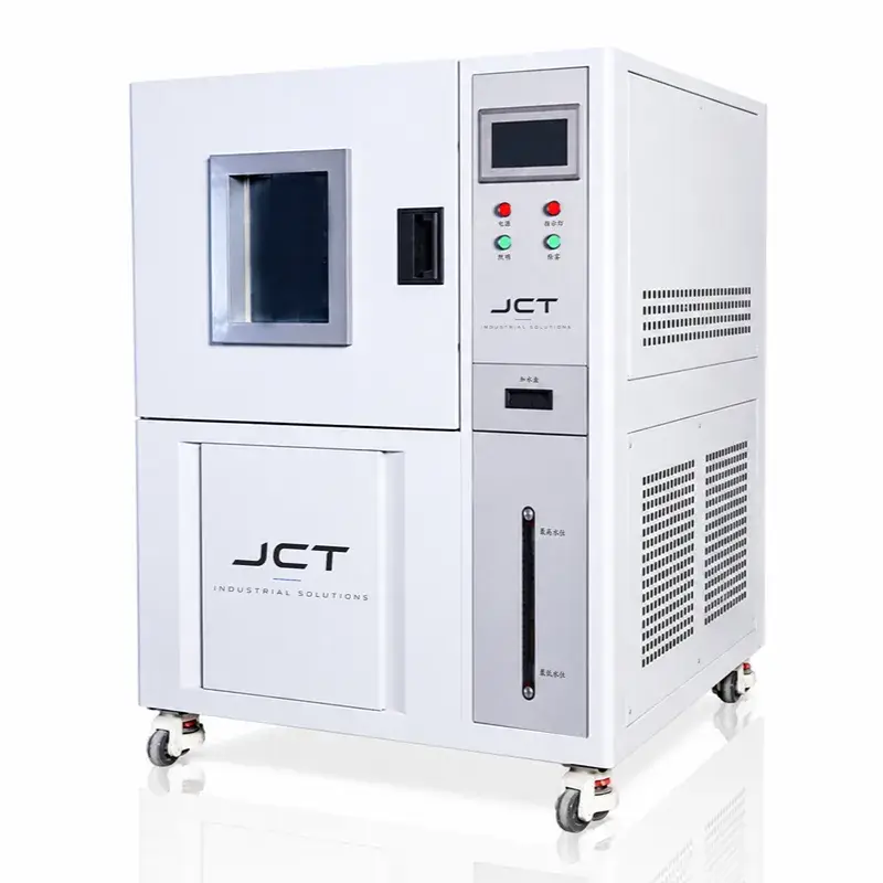
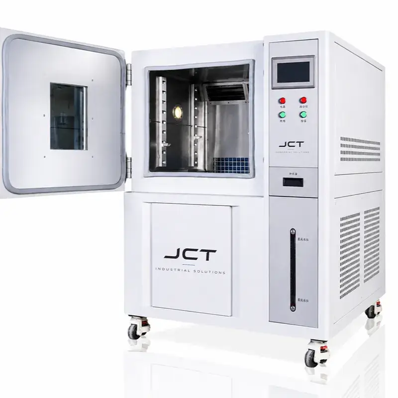
Delivers stable humidity control (±2% RH) . Features anti-condensation technology to prevent water droplets from pooling on delicate IC trays, and ensure pure vapor diffusion
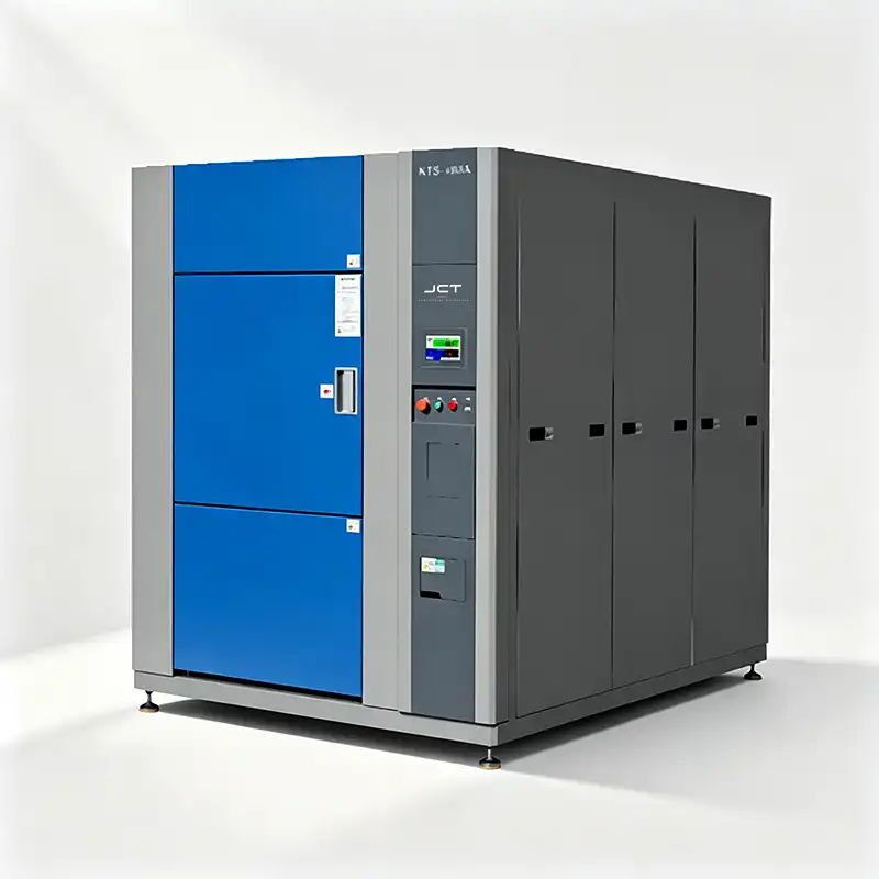
JESD22-A106 thermal shock testing, exposing wire bond shear, CTE mismatches, and die attach fracturing.
Maximum thermomechanical violence. The 2-Zone model uses a rapid pneumatic basket to transfer IC trays from -65°C to +150°C in under 10 seconds. The 3-Zone model utilizes damper technology for testing that requires a static ambient resting phase. Both of them provide lightning-fast temperature recovery times critical for JEDEC compliance.
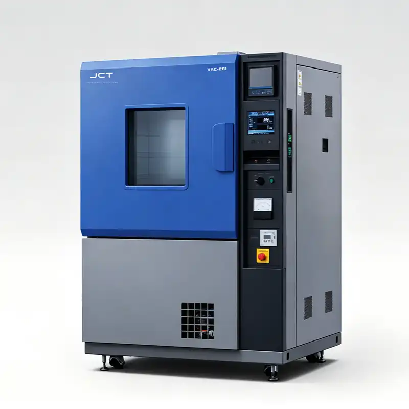
High-Temperature Storage Life (HTSL), static and dynamic burn-in testing, and accelerated aging of silicon wafers.
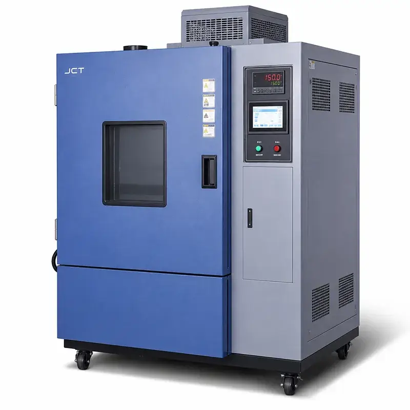
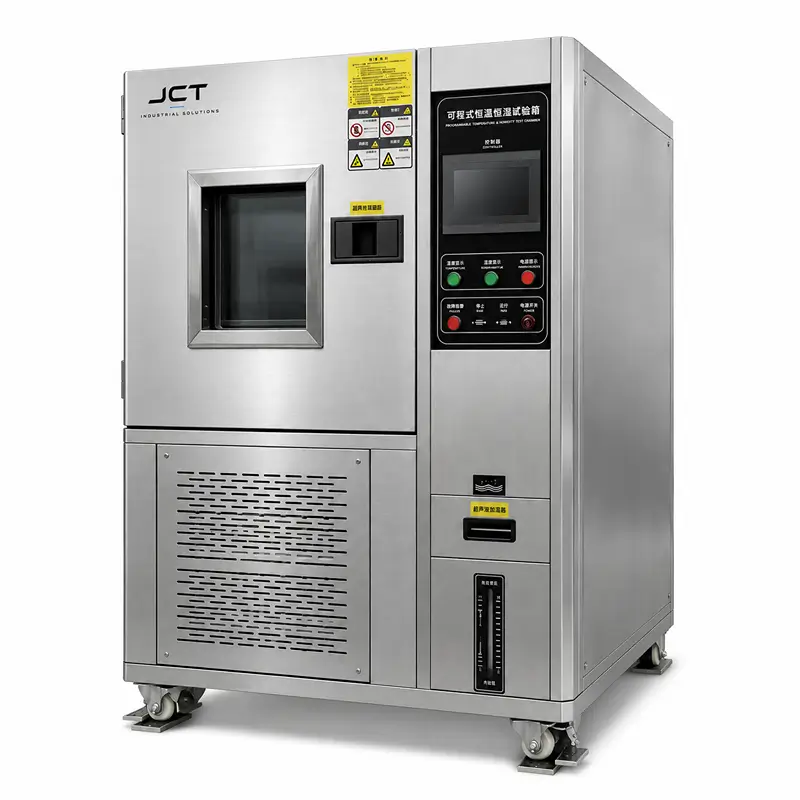
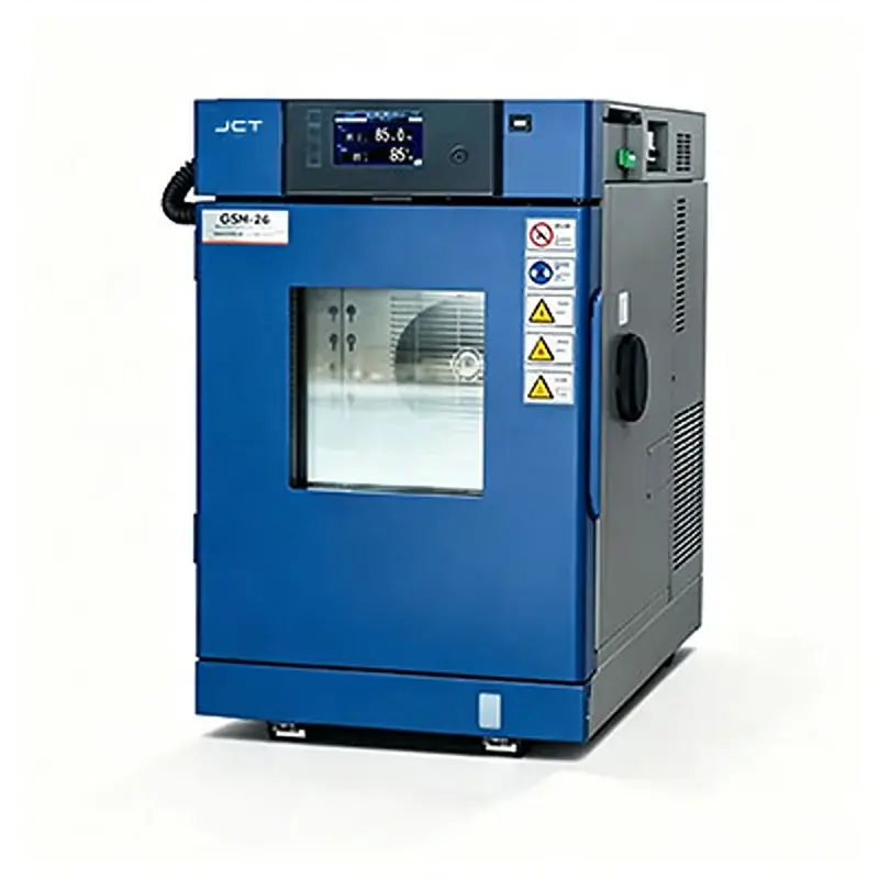
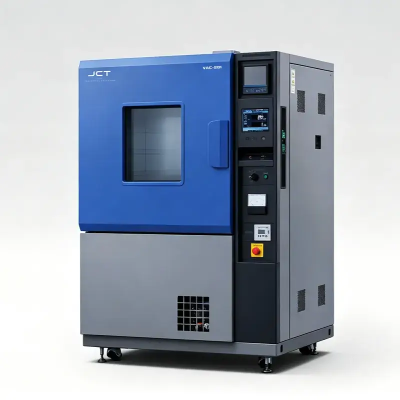
Engineered for extreme thermal stability (up to +300°C) . Built to safely accommodate heavy burn-in boards plugged with thousands of ICs. Features specialized exhaust ports to handle off-gassing from epoxies during curing and high-temperature stabilization bakes
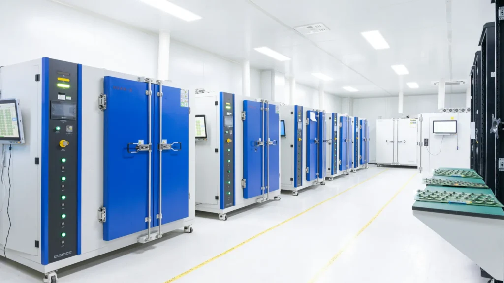
Direct Manufacturer of Environmental Test Chambers
WHO WE ARE?
We build environmental test chambers. We help you test raw materials and finished products under extreme conditions. We find potential quality risks before mass production, protecting your products from costly returns.
With over 10 years of industry experience, we cover a full range of equipment: +180℃ high temperature, -70℃ to +180℃ temperature & humidity, thermal shock, and salt spray corrosion chambers.
We have strong R&D and manufacturing power. We accept custom orders to match your exact test standards.
We hold over 30 patents. We are ISO9001 and CE certified. Our products are exported to 50+ countries, including Europe, North Europe, Australia, Latin America, and Southeast Asia.
We are the direct source factory—no middlemen. Choose JCT, and let us safeguard your product quality.
We hold multiple product patents. We are ISO9001 and CE certified.
Choose JCT. Choose a lifelong partner.
OUR CORE ADVANTAGES
Why Choose Us
With over 10 years of rich industry experience, we are committed to served as a comprehensive technology manufacturer partner worldwide.We understand that your successful product relies on two core pillars: efficient manufacturing and uncompromising quality control.As a result, we offer a dual-core product line: first, laser and FAB solutions that ensure efficient manufacturing; and second, environmental test chambers for testing the performance of your products—all designed to address your specific industry issues and challenges.

Industry-Specific Customization
Whether you’re in the sheet metal or metalworking industries, or specialize in testing semiconductors and automotive electronics, our equipments all can be customized to meet your specific needs. We don’t just sell standard machines—we provide precise solutions that perfectly match your material and environmental requirements.
High-Efficiency Manufacturing
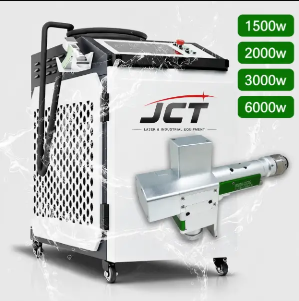
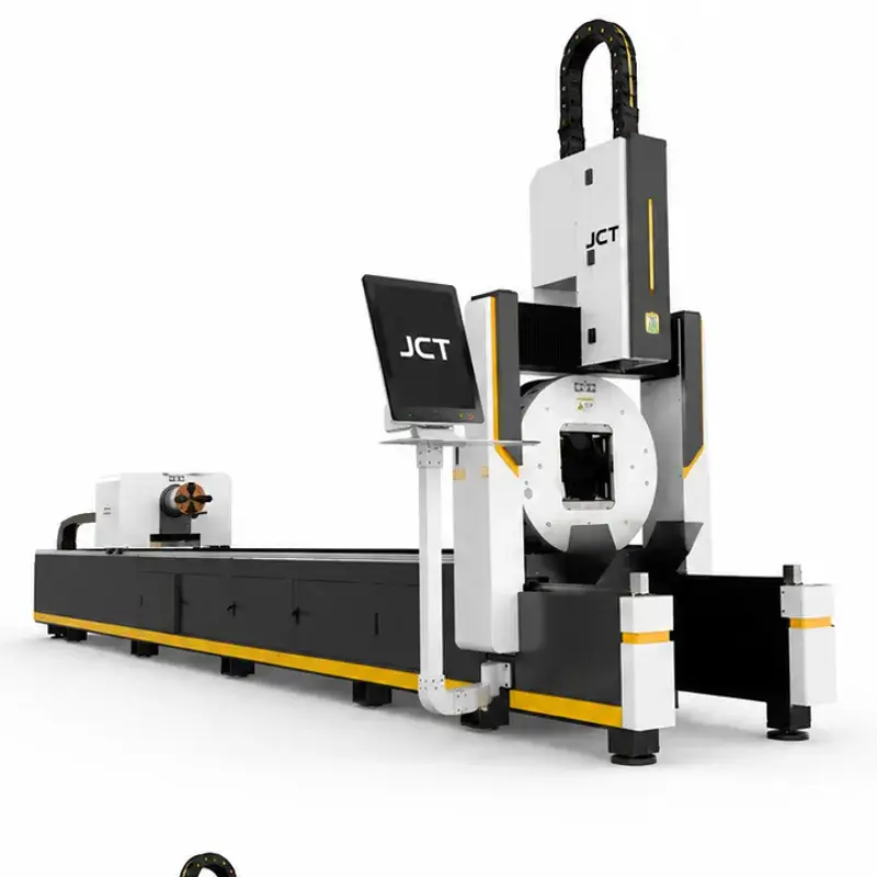
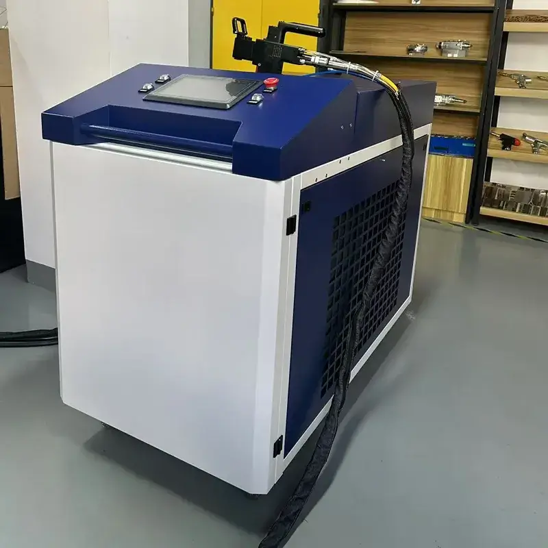
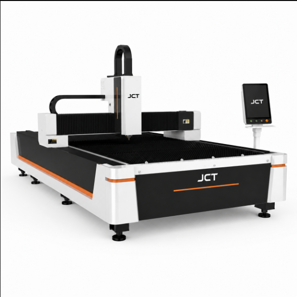
In the manufacturing process, time is your most valuable treasure. We offer fiber laser welding, cutting, and cleaning,etc solutions . All of them can provide deep penetration, distortion-free welding, precise cutting, and efficient cleaning for sheet metal and various types of metal processing.
Compliance and Quality Control
We ensure that your finished products can pass the most rigorous environmental testing. Our environmental test chambers help you meet strict global standards such as JEDEC, AEC-Q100, and key battery safety certifications, all these can shorten your R&D cycle and eliminating the risk of customer returns .
10+ Years & Global Support
With over a decade of technical expertise and a robust supply chain, we guarantee on-time delivery worldwide. More importantly, our engineering team will provide lifetime technical support, and we are committed to being your stable and reliable partner and friend for life.
PREMIUM COMPONENTS ASSURANCE
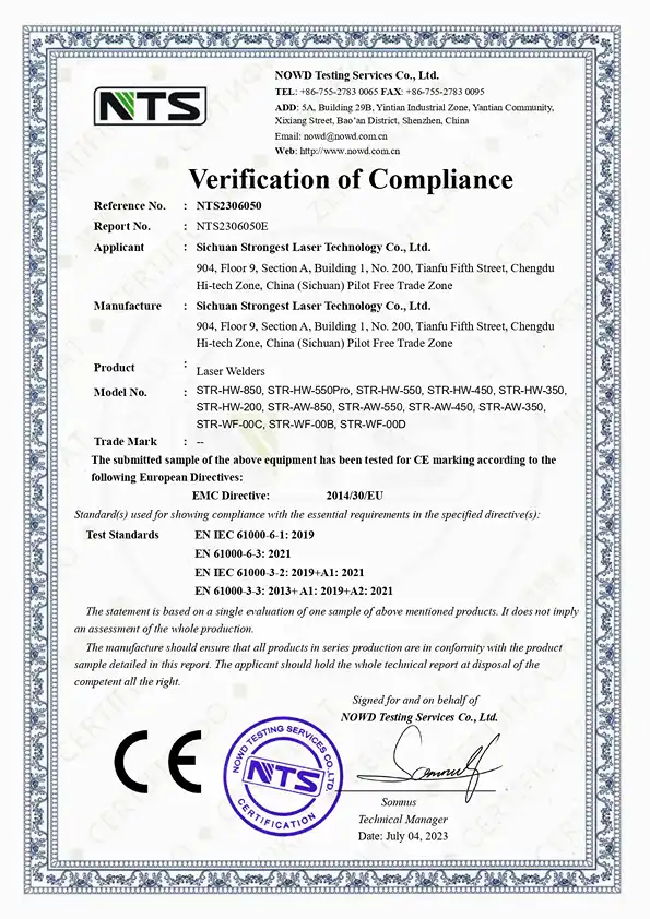
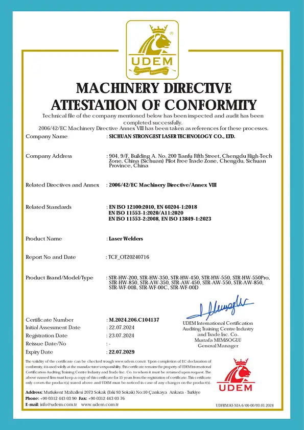
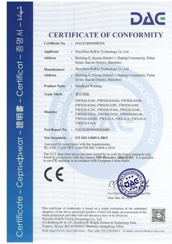
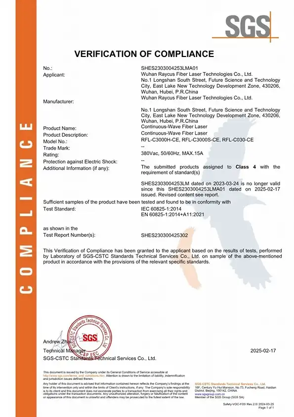
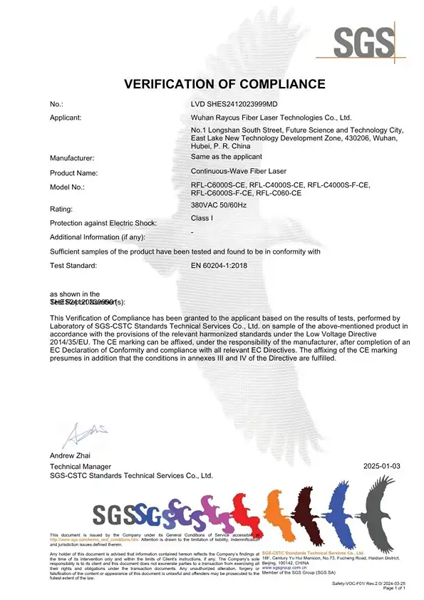
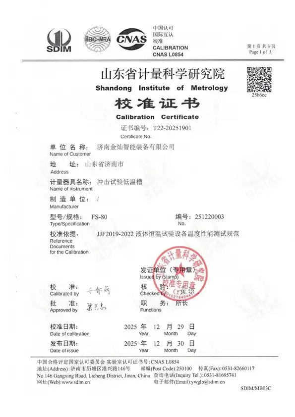
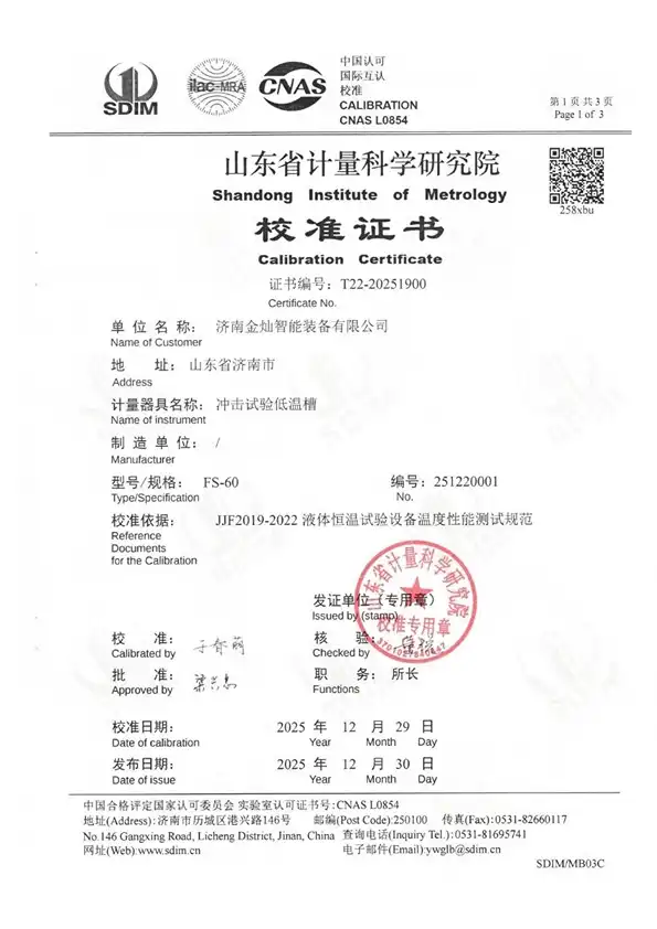
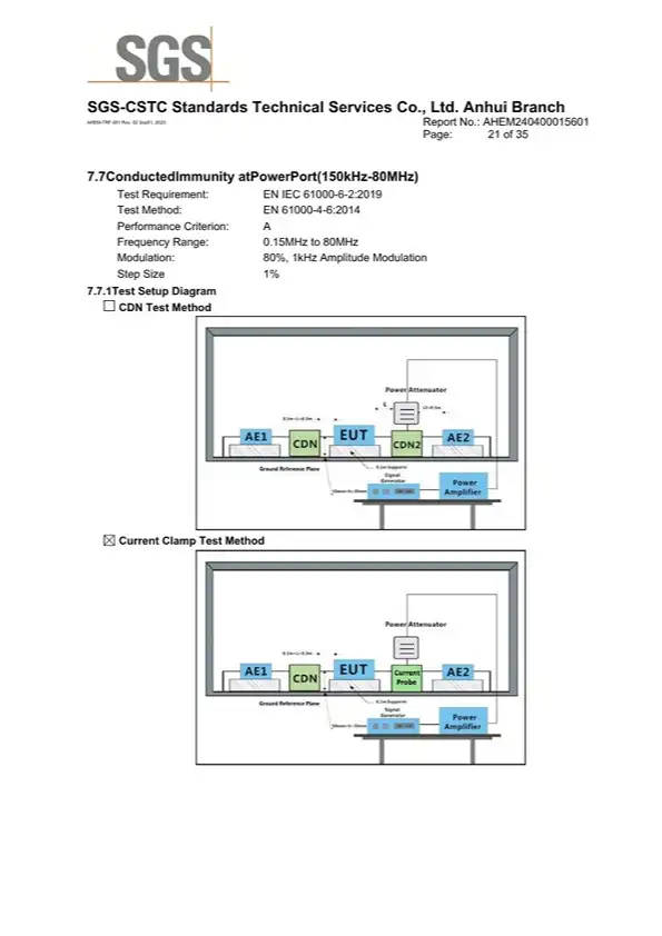
Certified to Global Leading Standards
Reliability starts at the core. The key components that power our equipment—from the laser source to even the smallest electronic components—have all been certified to meet the world’s most stringent international standards.
GLOBAL PARTNERSHIPS
Trusted by Industry Leaders Worldwide
We take pride in powering the success of top-tier global manufacturers, research institutions, and industrial leaders. Our advanced laser and testing solutions are trusted worldwide to deliver uncompromising quality and peak performance.














FAQ
Q1: Why do we need a humidity chamber if the chips will just be soldered on a dry SMT line?
Because microchips stay on shelves before they are soldered. The epoxy packaging absorbs moisture from the ambient factory air during storage. If you don’t use a humidity chamber to simulate this “floor life” absorption (MSL preconditioning), you will not know if your chips will explode (popcorn effect) when they hit the 260°C reflow oven.
Q2: What is the difference between testing in a Rapid Temp Change chamber versus a Thermal Shock chamber?
Rapid Temp Change ramps the temperature up/down linearly (e.g., 15°C/min) in a single zone; it tests thermal fatigue over time.
Thermal Shock mechanically moves the chips between a pre-heated zone and a pre-cooled zone in seconds. Thermal shock is far more violent and is specifically used to snap weak wire bonds and expose severe CTE mismatch.
Q3: For JEDEC thermal shock testing, should we use a 2-Zone or a 3-Zone chamber?
2-Zone: Moves the product directly from Hot to Cold (and vice versa) using a basket. It provides the most extreme, instantaneous shock.
3-Zone: The product stays stationary while hot, cold, or ambient air is blown in via dampers. It is required if your test standard dictates an “ambient dwell” phase between the hot and cold extremes
Q4: Can we run power cables into the High-Temperature chamber for dynamic burn-in testing?
Absolutely. We provide specialized, thermally sealed access ports on the sides of the chambers. This allows you to route heavy wiring harnesses and test probes from your external electrical cyclers directly to your burn-in boards without compromising the chamber’s temperature stability.
Q5: Can the chamber controllers output test data for our quality audit reports?
Yes. The advanced touchscreen controllers feature massive onboard memory and USB export functionality. Furthermore, they are equipped with RS-485 and Ethernet TCP/IP ports, allowing them to integrate directly into your factory’s MES or central lab software for real-time, unalterable data logging.
Q6: What maintenance is required for a Thermal Shock chamber?
The primary maintenance involves cleaning the condenser fins of the refrigeration system, ensuring the pneumatic system driving the transfer basket is lubricated and free of moisture , and annually calibrating the temperature sensors .
Q7: What is the lead time for these specialized semiconductor testing chambers?
Standard chambers (Constant Temp/Humidity and High Temp) generally have a lead time of 4 to 6 weeks. Highly complex 2-Zone or 3-Zone Thermal Shock chambers, due to their intricate cascade refrigeration and pneumatic systems, typically require 8 to 10 weeks for manufacturing, testing, and calibration.
Related Products
Get a Factory-Direct Custom Quote
Do not let the popcorn effect or thermal fatigue destroy your semiconductor yields.
Tell our environmental engineering team about your specific IC packages (e.g., BGA, QFN, SiP), required JEDEC testing standards, and desired payload volume. We will recommend the exact, highly-precise JCT testing chamber to secure your OSAT and foundry quality, complete with a factory-direct quote within 12 hours.